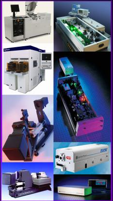
 The focus of this research group is the measurement of nanoscale properties including dimensions. Metrology, the science of measurement, covers a wide range of techniques and thus physics. As the dimensions of nanoelectronic features shrink, phenomena such as quantum confinement alter the physical properties of materials and the measurements of nanoscale materials. In addition, interface properties are often determining factors in the function of nanoscale materials stacks and structures. This group covers all areas of nanometrology and specializes in linear and non-linear optical measurements and electron microscopy.
Dr. Diebold’s group works in the field of nanoelectronic metrology. His research interests include:
- Metrology for CMOS extension including transistor and interconnect metrology. This includes all measurement areas: thin film, stress, feature shape and dimension.
- Characterization and Metrology for Beyond CMOS Devices.
- The optical physics of nano-scale materials and measurements.
- Linear and Non-linear optical measurements of interfacial properties.
- Optical characterization of quantum confinement, excitons, and other phenomena in nanoscale materials and structures.

