CHIPS act at the AVS 69 National Symposium
There will be a special session on the CHIPS act at the AVS 69 National Symposium in Portland, OR hosted by the Manufacturing Science and Technology Group. You can find the most up to date details at https://avs69.avs.org/
2024 Frontiers of Characterization and Metrology for Nanoelectronics
The 2024 Frontiers of Characterization and Metrology for Nanoelectronics will be held in Monterey, CA. Conference co-chairs are J. Alex Liddle, Paul van der Heide (IMEC), Markus Kuhn (Rigaku), Zhihong Ma (INTEL), and Alain Diebold (CNSE)
International Conference on Spectroscopic Ellipsometry
The International Conference on Spectroscopic Ellipsometry 10 will be held in Boulder CO in the summer of 2025. The conference co-chairs are Mathias Schubert (U. Nebraska), David Aspnes (NCSU), and Alain Diebold (CNSE).
POD CAST on Semiconductor Characterization and Metrology
Markus Kuhn recently interviewed Alain Diebold for a Pod Cast on Understanding Semiconductors. This Pod Cast provides an early look at semiconductor characterization and metrology at SEMATECH and how it evolved along with the industry. https://rsmd.rigaku.com/newsnusecases/professor-alain-diebold-ph.d.-successes-at-sematech-effective-approach-to-metrology-challenges-and-key-takeaways-from-2022-fcmn-conference
AVS Hudson Mohawk Chapter
Dr. Alain Diebold is a member of the AVS - Hudson Mohawk Chapter. https://avs.org/about-avs/chapters/avs-regional-chapters/hudson-mohawk/meet-a-member-(alain-diebold)/
New Book titled Optical and Electrical Properties of Nanoscale Materials
Optical and Electrical Properties of Nanoscale Materials (published in December, 2021) by Springer Nature. The book provides an overview of 2D materials including graphene, transition metal dichalcogenides, and topological materials. Many derivations are provided in detail. The authors are Alain Diebold and Tino Hofmann (UNC). https://link.springer.com/book/10.1007/978-3-030-80323-0
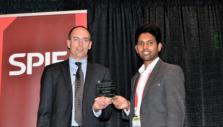
The Diana Nyyssonen Memorial Best Paper Award 2020/21 Winner at SPIE Advanced Lithography 2021
Congratulations to The Diana Nyyssonen Memorial Best Paper Award 2020/21 Winner: X-ray metrology of nanowire/ nanosheet FETs for advanced technology nodes, Madhulika Korde, R. Joseph Kline, Daniel F. Sunday, Nick Keller, Subhadeep Kal, Cheryl Alix, Aelan Mosden, Alain C. Diebold, Proceedings Volume 11325, Metrology, Inspection, and Process Control for Microlithography XXXIV; 113250W (2020) https://doi.org/10.1117/12.2553371 (edited)
Springer
Dr. Diebold is an editor for a new series titled SpringerBriefs in Materials.
Research highlighted in Semiconductor Engineering
Our research on Mueller Matrix spectroscopic ellipsometry and CD-small angle X-ray scattering discussed in Semiconductor Engineering article on metrology for gate –all-around transistors.
ICSE 8 Barcelona
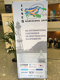 |
The International Conference on Spectroscopic Ellipsometry 8 was held in Barcelona at the World Trade Center from May 26 to 31, 2019. The conference was chaired by M Isabel Alonso and multiple International Organizing Committees. https://congresses.icmab.es/icse8/
The more than 300 attendees came from around the world. Tutorials were held on Sunday May 26 as well as a heart-felt session remembering the countless contributions of Manuel Cardona. Both optical properties of new materials such as 2D (Transition Metal Dichalcogenides) and metal oxides (Ga2O3) and equipment (pump – probe ellipsometry and ellipsometry microscopes) were discussed. The Drude award was shared by Eva Bittrich for research in organic and polymer thin films and interfaces and Chris Sturm for extending our understanding of excitonic and band-band transitions for all classes of crystals especially biaxial anisotropic materials. Previous Drude award winner have continued highly successful research efforts in spectroscopic ellipsometry.
Frontiers of Characterization and Metrology for Nanoelectronics – 2019
Monterey, CA April 1 -5, 2019
https://www.nist.gov/news-events/events/2017/03/frontiers-characterization-and-metrology-nanoelectronics
AVS 65th International Symposium & Exhibition
Long Beach, CA Oct. 18 -23, 2018
Focus Topic on Spectroscopic Ellipsometry
Focus Topic on Manufacturing Science and Technology
https://s19.a2zinc.net/clients/avs/avs18/public/enter.aspx
TOM 6 - Frontiers in Optical Metrology
European Optical Society Biannual Meeting, Oct. 8-12, 2018
http://www.myeos.org/events/eosam2018_tom6
 Sonal Dey meets New York State Congressman Paul Tonko at the A2 beamline at CHESS
Congressman Paul Tonko also serves as a member of the Science, Space and Technology Committee, and the subcommittee on Research and Technology, which has jurisdiction over non-defense federal scientific research and development. Sonal demonstrated to Congressman Tonko the growing need of using a national synchrotron facility like CHESS in elucidating the physicochemical properties of thin film structures, and nanoscale patterned wafers which are being researched for use in next generation semiconductor chips, computers, cell phones, and internet of things, to name a few. For more information on Congressman Paul Tonko’s visit to CHESS and subsequent interaction with the scientific community, visit http://news.chess.cornell.edu/articles/2016/Ryan161111.html.
 Avery J. Green’s article selected as Editor’s Pick by JVSTA
His recent work, entitled Surface oxidation of the topological insulator Bi2Se3, was selected by the Journal of Vacuum Science & Technology A for its application to the rapidly growing field of topological materials. The article constitutes a multi-experimental approach to measuring the time-dependent surface quality of Bi2Se3. (Link)
Journal of Vacuum Science & Technology A publishes reports of original research, letters, and review articles that focus on fundamental scientific understanding of interfaces, surfaces, plasmas and thin films and on using this understanding to advance the state-of-the-art in various technological applications. More information about JVSTA can be found at http://scitation.aip.org/content/avs/journal/jvsta.
 Sonal Dey featured in CHESS newsletter for metrological work on ALD higher-k dielectrics
His work, now featured in the publication, Role of Ge and Si substrates in higher-k tetragonal phase formation and interfacial properties in cyclical atomic layer deposition-anneal Hf1−xZrxO2/Al2O3 thin film stacks, utilizes the CHESS synchrotron source to create high-resolution x-ray diffraction maps. This collaboration provides invaluable information about the orientation, phase, composition, and stress of ultrathin layer stacks. CHESS recognized this work for its high scientific quality, and importance to materials science applications in the semiconductor community.
CHESS is a high-intensity X-ray source supported by the National Science Foundation which provides our users state-of-the-art synchrotron radiation facilities for research in Physics, Chemistry, Biology, and Environmental and Materials Sciences. A special NIH Research Resource, called MacCHESS, supports special facilities for macromolecular crystallography and BioSAXS. CHESS-U is the current upgrade that will extend CHESS’s capacity for cutting edge research. For more information on CHESS, visit http://www.chess.cornell.edu/.
Avery J. Green earns award for best student presentation in Spectroscopic Ellipsometry at the 62nd annual AVS Symposium
His presentation, entitled “Structural and ellipsometric analysis of the topological insulator Bi2Se3″ was selected as the best student talk in the focus topic of Spectroscopic Ellipsometry at the 62nd annual AVS Symposium in San Jose, CA.
The AVS International Symposium and Exhibition addresses cutting-edge issues associated with materials, processing, and interfaces in the research and manufacturing communities. The weeklong Symposium fosters a multidisciplinary environment that cuts across traditional boundaries between disciplines, featuring papers from AVS technical divisions, technology groups, and focus topics on emerging technologies. The equipment exhibition is one of the largest in the world and provides an opportunity to view the latest products and services offered by 200+ participating companies. More than 2,000 scientists and engineers gather from around the world to attend.
For more information on the conference, visit https://www.avs.org/symposium
 Dhairya J. Dixit earns award for best student paper of 2014 at the Advanced Semiconductor Manufacturing Conference (ASMC)
His paper, entitled “Mueller Matrix Optical Scatterometry of Si Fins Patterned using Directed Self-Assembly Block Copolymer Line Arrays” was recognized by the ASMC technical committee for its experimental and analytical quality, as well as its value to the semiconductor community.
ASMC continues to be one of the leading international technical conferences for discussing solutions that improve the collective manufacturing expertise of the semiconductor industry. Solving the challenges presented by semiconductor manufacturing has been a combined effort by device makers, equipment and materials suppliers and academics. Technical presentations at ASMC highlight industry innovations with specific results.
For more information on the conference, visit http://www.semi.org/node/38316
Dr. Alain Diebold, CNSE Empire Innovation Professor of Nanoscale Science recognized as a SPIE Fellow at SPIE Advanced Lithography Conference, San Jose,CA (2013)
He is one of only 69 members of distinction to earn the honor in 2013, which highlights technical achievements and service to the general optics community, as well as service to the society.
Known as the world’s leading nanoelectronics lithography conference and exhibition, the 39th annual SPIE Advanced Lithography conference was held in February 24 through 28 in California at the San Jose Convention Center.
For more information on the conference, visit spie.org
CNSE Student G.Raja Muthinti won the Best Paper Award in Metrology, Inspection, and Process Control for Microlithography XXVII at SPIE Advanced Lithography Conference, San Jose, CA (2013)
A panel of judges from academia, industry, and government honored him during a ceremony for his research paper, “Mueller-based scatterometry measurement of nanoscale structures with anisotropic in-plane optical properties,” based on technical merit and presentation quality.
Muthinti, who is from Vishakapatnam, India, is currently pursuing PhD in Nanoscale Engineering at CNSE.
Award ceremony at the SPIE conference, visit Best Paper Award:Video
 CNSE Student Lay Way Kong won second prize for her poster paper at the 11th International Workshop on Stress-Induced Phenomena in Metallization April 12 – 14, 2010 in Dresden, Germany.
This work titled “Sub-imaging techniques for 3D-interconnect on bonded wafer pairs” is a collaboration between CNSE, SEMATECH and the Fraunhofer Institute for Nondestructive Testing Dresden (IZFP-D).
The workshop provided a forum for presenting current research and for discussions on issues related to stress-induced phenomena in on-chip metal interconnects and solder joints. Stresses arising in metal structures and surrounding dielectric materials due to novel process steps, thermal mismatch of thin film materials, electromigration or microstructure changes can lead to degradation and failure of microelectronic products.
The implementation of low dielectric constant materials into the inlaid copper backend-of-line process has brought new challenges for process integration, design optimization and reliability. Understanding stressrelated phenomena in new materials and structures is critical for development and integration of future metal structures in microelectronic products.
