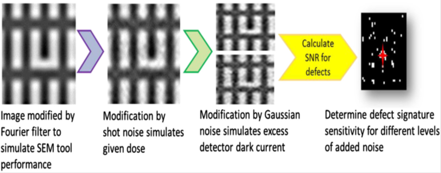
As the feature sizes in microelectronics devices continue to shrink, the specifications for manufacturing quality control become increasingly demanding. As a general rule, the size of a critical defect in a patterning step is half of the feature size of the technology node. Thus for a so-called 7 nm technology chip, the critical defect size is 3.5 nm. Scanning electron microscopy has long been a standard method for measuring critical dimensions on patterned wafers (the CD-SEM), but now there is increased interest in using electron beam technologies for pattern defect inspection. Our work uses a combination of simulations and experiments on reference standards to consider how the electron-optical performance of the SEM impact CD measurement of complex architectures and sensitivity to defects.