Research Examples
- Design and Economic Considerations to Achieve the Price Parity of SiC MOSFETs with Silicon IGBTs
- Area-Efficient Bevel-Edge Termination Techniques for SiC High-Voltage Devices
- Development of 1.2kV rated SiC MOSFETs with accumulation mode channel and inversion mode channel
- Monolithically Integrated 4H-SiC MOSFET and JBS Diode (JBSFET) using a Single Ohmic/Schottky Process Scheme
- Edge termination techniques for high voltage devices (3.3kV and 4.5kV) on SiC
Recent Projects
- Integrated SiC MOSFET and JBS diode – PowerAmerica BP-1;
- Novel edge termination for high voltage SiC devices – PowerAmerica BP-1;
- Foundry Process Kit for 1.2kV SiC Power MOSFETs and JBS Rectifiers – PowerAmerica BP-2;
- Development of 6.5kV/10kV SiC MOSFETs, JBS Diodes, and JBS Diode Integrated MOSFETs –PowerAmerica BP-3;
- 600V SiC Lateral & Vertical JBS Diodes and MOSFETs – PowerAmerica BP-3;
- Manufacturing of Ultra-high-voltage SiC devices (MUSiC) – Army Research Lab / Office of Naval Research;
- Scalable, Manufacturable, And Robust Technology for SiC Power Integrated Circuits (SMART SiC Power ICs) – ARPA-e/DOE;
- CPR (Cost competitive / high-Performance / highly Reliable) Power Devices on SiC and GaN – VTO/DOE;
- Power Nitride Doping Innovation Offers Devices Enabling SWITCHES (PNDIODES) – ARPA-e/DOE;
- Improving SiC Wafers and Processing for Lower Costs and Higher Reliability – AMO/DOE;
- Others: Projects with Companies.
TOPIC 1: Design and Economic Considerations to Achieve the Price Parity of SiC MOSFETs with Silicon IGBTs [1, 2]
In 2015, U.S Department of Energy has launched an Institute (PowerAmerica) under the initiative of National Network of Manufacturing Institutes (NNMI) to commercialize Wide Band Gap (WBG) power devices. One of the primary goals of the Institute is to achieve significant reductions in the cost of manufacturing WBG devices and achieve price parity with Si IGBTs in the 600 – 1700 V range within 5 years of its inception and fall below today’s Si prices in 5-8 years. SiC is considered as a post-silicon device for power electronics applications because its superior material properties guarantee low power losses, higher efficiency, and smaller system volume and weight. Since the advent of the first SiC SBD in the 1990’s, numerous research groups devoted efforts to commercialize SiC devices, such as MOSFETs, JFETs, BJTs, and thyristors. However, it is believed that massive adoption of SiC power devices will not take place until there are substantial improvements in two major barriers: reliability, and price.
The most effective way of achieving price parity to Silicon counterparts is to reduce the material cost that contributes to about 50% of the overall SiC chip cost. Development of large diameter substrates to enhance yield are being pursued by wafer and chip manufacturers. On top of these efforts, device innovation not only brings chip size reduction, but also directly brings material cost reduction. However, there is a lack of quantitative analysis to suggest direction regarding improvement and consequent cost projections.
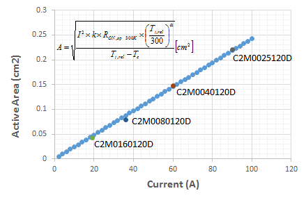
In this research, methodologies to reduce the chip size of SiC MOSFETs are discussed based on an analytical-empirical model by examining temperature coefficient, junction temperature, on-state resistance, thermal resistance of the package, and edge termination techniques (Fig. 1). In the analysis of chip size, reliability is also taken into consideration because these two factors are mutually related in some aspects. Analyses based on the developed model, lead to following conclusions; Even 5 times higher channel mobility of the planar SiC MOSFET can only save 13% of the active area because the temperature coefficient is also increased close to that of SiC bulk resistor; The development of packaging technology to lower the thermal resistance becomes an effective way of reducing the size of the chip; Edge termination and periphery area must be reduced to achieve chip-scale reduction in size. This analysis justifies the advanced packaging technologies, such as double-sided cooling, and flip-chip technique.
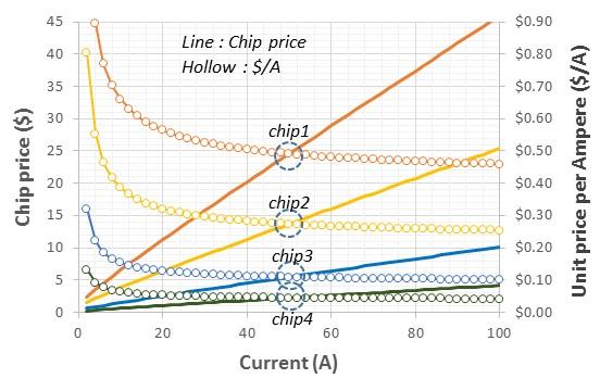
Finally, the cost analysis based on the proposed model clearly illustrates how the price parity to the Silicon IGBTs can be achieved. Other than the device innovation, from an exemplary cost analysis, it is found that wafer price, process yield, and wafer size also play significant roles in reducing the chip price (see Fig. 2, and Table 1). Improvement in each parameters discussed in this research should be pursued in parallel to lead to price-parity to silicon devices.
 |
 |
|
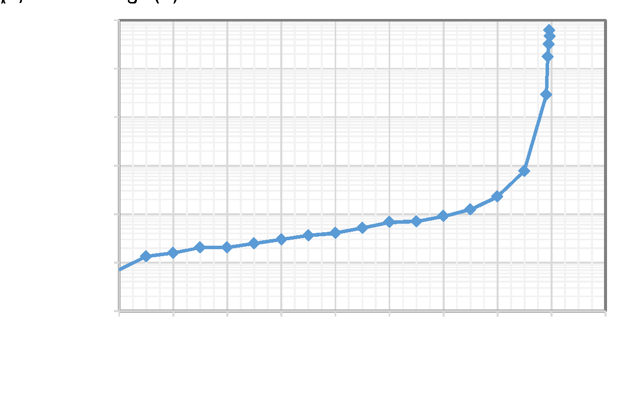
Fig. 1. Active area to target specific currents based on the proposed model (inset). Commercial 1200V SiC MOSFET information are also plotted, and well matched with the model. |
Fig. 2. 1200V SiC MOSFET price projection. Conditions in Table 1 were used in this analysis. |
TOPIC 2: Area-Efficient Bevel-Edge Termination Techniques for SiC High-Voltage Devices [3]
In recent years, significant improvements in performance have been achieved in SiC devices, such as MOSFETs, BJTs, JFETs, IGBTs, GTOs, JBS, and PiN Diodes. In these high voltage SiC vertical devices, one of the major design concerns is the edge termination. Floating Field Rings (FFRs), or Junction Termination Extension (JTE) -based structures are commonly used edge termination approaches. However, those conventional edge termination techniques consume a significant amount of area on the chip. As a rule of thumb, the edge termination width has dimensions equal to ~5 times the drift region thickness. To reduce the chip size, and thus the cost of the SiC chip, area efficient edge termination techniques are an imperative.
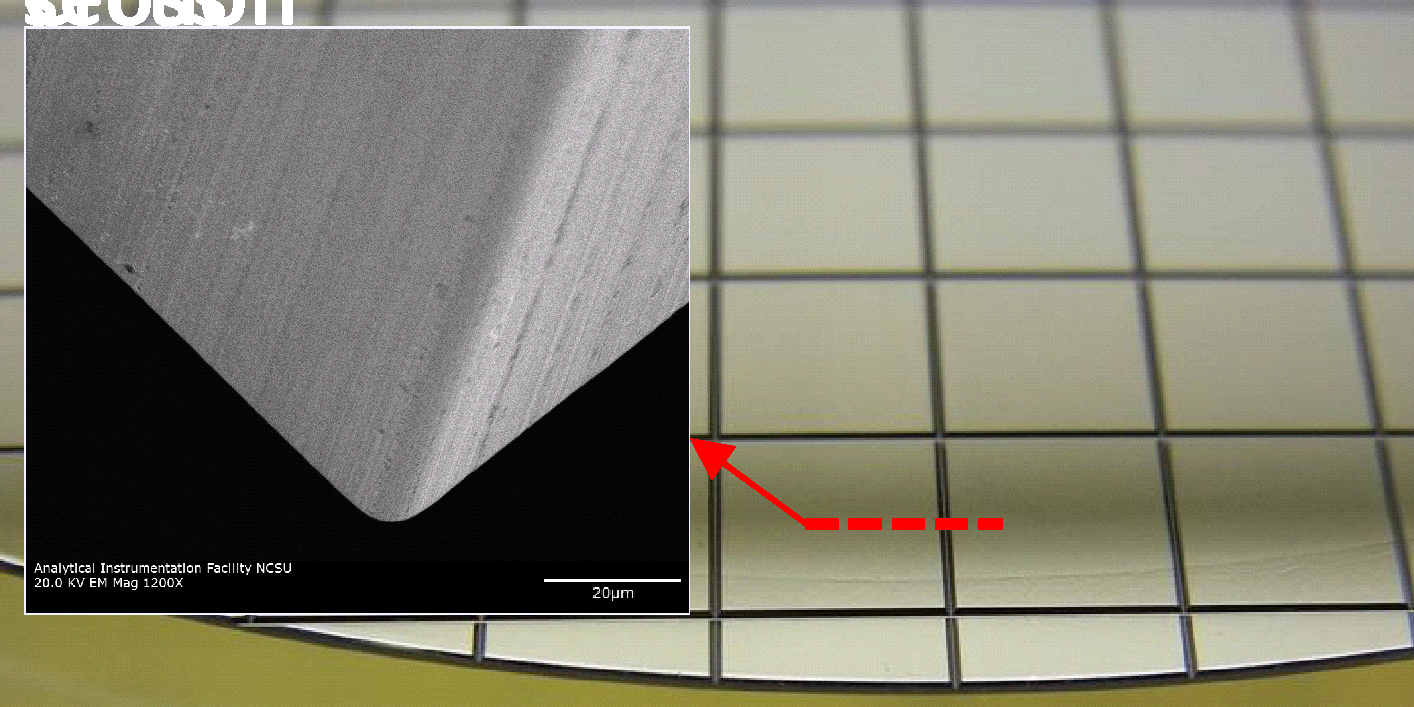
Orthogonal positive bevel edge termination technique has been proposed to produce symmetric blocking structures in SiC. It has been successfully demonstrated that a chip-scale bevel edge termination becomes feasible by using a V-shaped dicing blade as shown in Fig. 3. This technique was successfully demonstrated to achieve high blocking voltage at the substrate-drift layer junction. The bevel edge termination can also be applied to support high voltage at the top PN junctions.
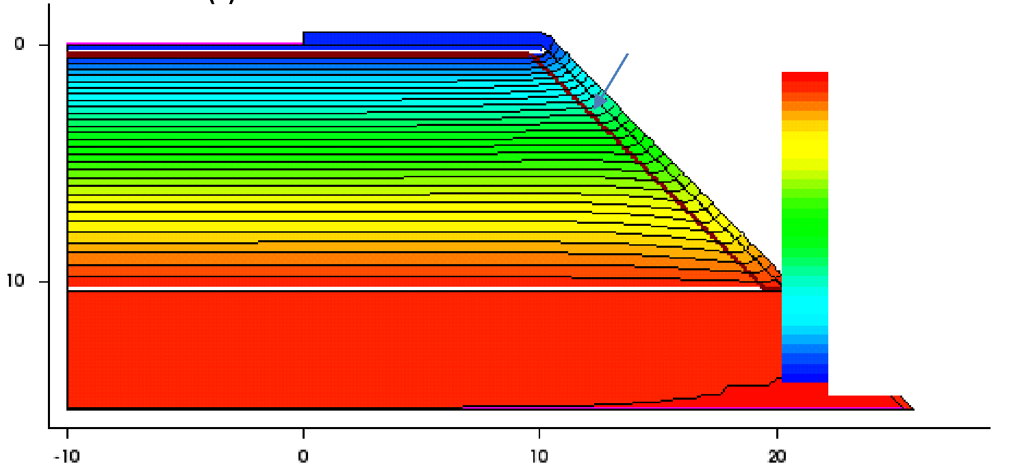
In this study, various innovative edge termination structures using the bevel technique, such as Bevel Junction Termination Extension (Bevel-JTE), Resistive Bevel Termination (RBT), Bevel Assisted JTE (BA-JTE), Positive Bevel Termination (PBT) were investigated. A cross-sectional view of the Bevel-JTE is shown in Fig. 4 as an example. Device simulation shows a uniform distribution of potential within the Bevel-JTE structure (Fig. 5). The aforementioned non-planar, 3D edge termination techniques significantly reduce the chip size because they require only 1X of the epi-layer in width on the SiC surface.
In general, bevel edge terminations have very low leakage current because the high hardness of SiC smooths the surface morphology when rubbed by the dicing blade (see the I-V curve in Fig. 6). Any residual damage can be then removed by RIE. It should be noted that the Bevel-JTE structure does not even require a photolithography step; CVD oxide, or other properly chosen materials, can be deposited before the dicing step. They can serve as a masking layer for the SiC surface etch treatment process and the JTE ion implantation step. After the bevel groove is inscribed on the wafer, a spray coater can substitute the spin coater for subsequent photolithography processes. Groove filling using a proper dielectric material, followed by a planarization process, can also be a good alternative. Passivation of the bevel surface, and the effect of possible inclusion of negative or positive charges should be further studied.
Since the bevel edge termination is fabricated with a dicing blade, it can be applied to any vertical device in SiC that has a drift layer of different thickness by adjusting the dicing depth. In fact, it is more attractive to use the Bevel-JTE structure for higher voltage devices because a significantly larger area of the wafer is occupied by edge termination structures using conventional approaches. Using the bevel edge termination discussed in this research, significant area can be saved, which in turn contributes to chip cost reduction.
 |
 |
|
Fig. 3. Wafer image after bevel dicing. Scanning Electron Microscope (SEM) image of bevel surface with 45 degree blade is also shown. |
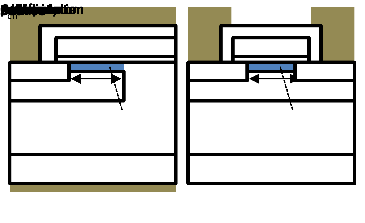
Fig. 4. Cross-sectional view of Bevel-JTE. JTE width for the conventional single-zone JTE is 50µm, while that of Bevel-JTE is about 15µm. |
 |
 |
|
Fig. 5. Potential contour of Bevel-JTE at 1720V. JTE dose in this simulation is 1×1013cm-2. |
Fig. 6. Typical reverse characteristics of fabricated PiN diodes with Bevel-JTE measured after N2O RTA process. Implanted JTE dose is 1×1013cm-2. |
TOPIC 3: Development of 1.2kV rated SiC MOSFETs with accumulation mode channel and inversion mode channel [4, 5]
In the past decade, there has been tremendous progress in the electrical performances of 4H-SiC power MOSFETs resulting in their commercialization. However, detailed information on the design of the channel to achieve a reasonable threshold voltage and field effect mobility is lacking in previous literature. Experimental results obtained on both accumulation mode channel design (AccuFETs) and inversion mode channel design (InvFETs) are compared in this research.
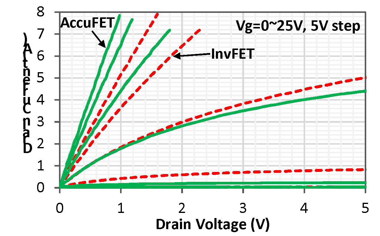
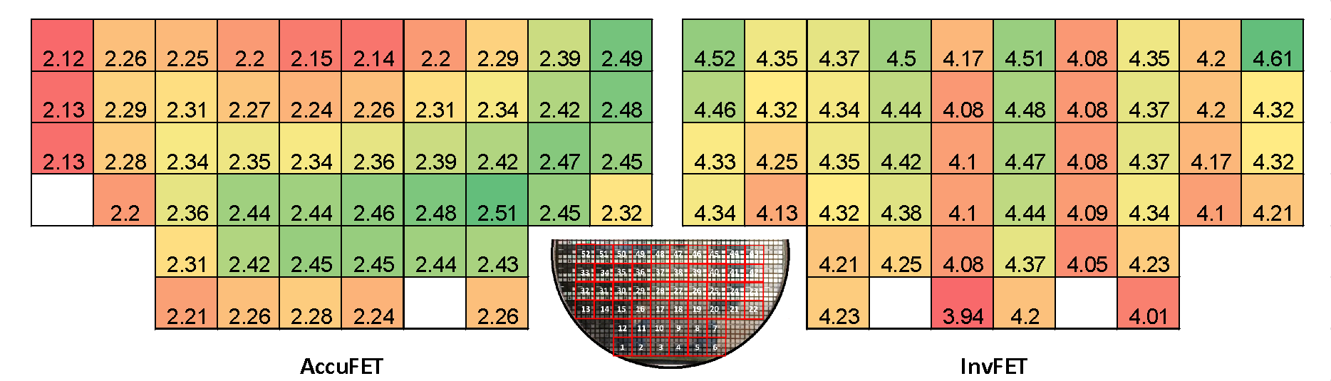
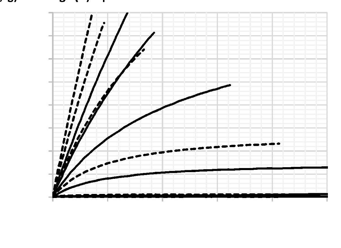
Fig. 7 shows cross-sectional diagrams of the 1.2kV SiC vertical power MOSFET and the lateral test structure used to extract the channel mobility. Doping profiles near the SiC surface were optimized by 2-D device simulations in order to accomplish reasonable threshold voltage with high channel mobility. The proposed MOSFETs were fabricated in a 6-inch wafer foundry company, XFAB, TX, U.S.A. Total 9-mask was used for fabrication of the AccuFETs and InvFETs. Fig. 8 shows on-wafer output characteristics of a typical AccuFET and InvFET. Specific on-resistances at drain current of 1A are 4.95 mΩ∙cm2, and 7.75 mΩ∙cm2, for the AccuFET, and InvFET, respectively, at a gate bias of 25V. The average threshold voltages out of 50 AccuFETs, and InvFETs at Id of 1mA are 2.33V, and 4.27V, respectively. Threshold voltages of both structures show tight distributions across the 6-inch wafer (see Fig. 9).
 |
 |
|
Fig. 7. Cross-sectional views of fabricated SiC Inversion mode and Accumulation mode MOSFETs (Lch=0.5µm), and lateral MOSFET (Lch=200µm) |
Fig. 8: Typical output characteristics of fabricated SiC AccuFETs and InvFETs. Active area: 4.5 mm2, measured at room temperature. |
 |
|
Fig. 9. Distribution of threshold voltages of SiC AccuFETs and InvFETs fabricated on 6-inch SiC wafers. A half-cut picture of a fully processed 6-inch wafer is also shown in the middle. Threshold voltages of AccuFETs show radial pattern across the wafer while those of InvFETs show random distribution. |
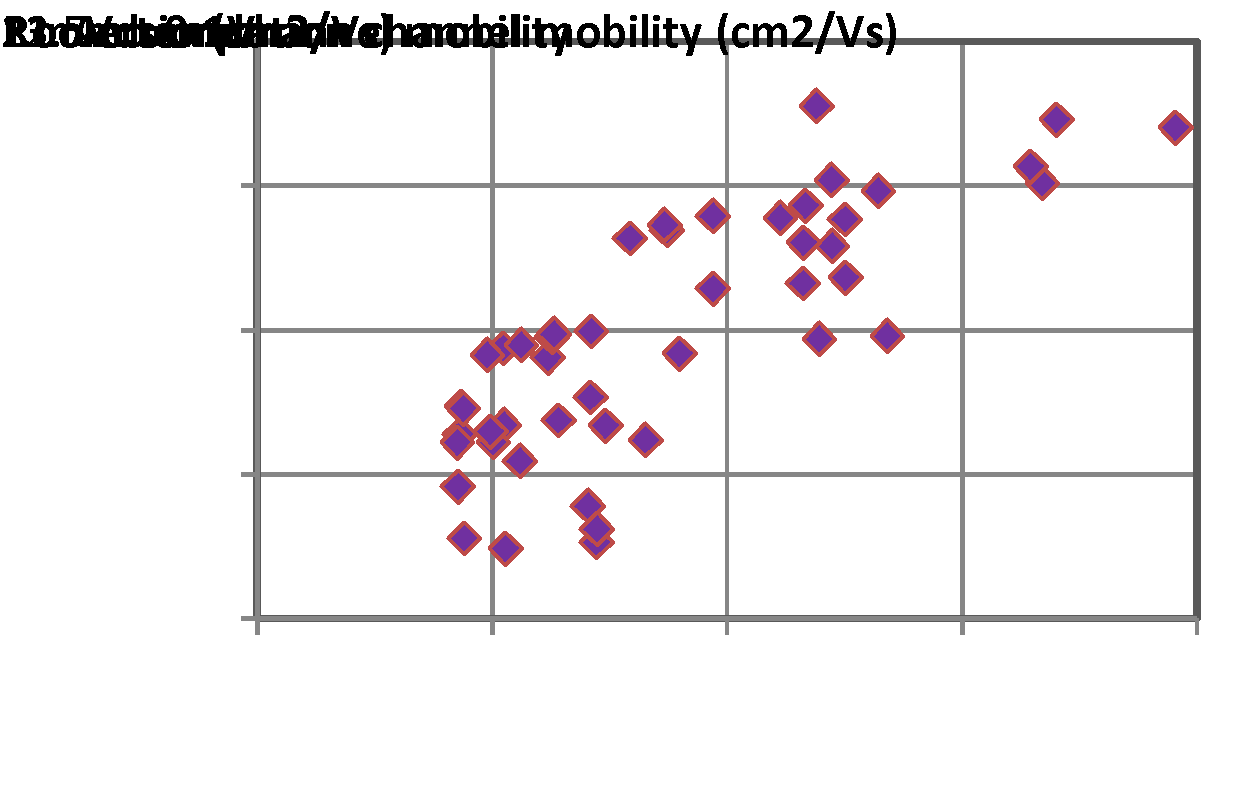
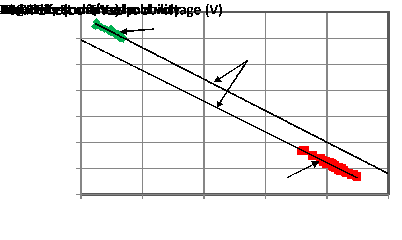
Field effect channel mobilities were calculated from transconductances measured on lateral MOSFETs with channel length of 200 µm. Fig. 10 shows a good correlation between the accumulation channel mobility and the inversion channel mobility, which may be attributed to common process variations such as the gate oxide thickness and the subsequent annealing. A clear correlation between the threshold voltage and the channel mobility was observed for both AccuFETs and InvFETs as shown in Fig. 11. This correlation is informative to establish the gate oxidation and post oxidation anneal (POA) process. Threshold voltages and channel mobilities at high temperatures were also compared (not shown in this report). It was also proven that no significant deterioration was produced in blocking characteristics by both channel designs.
In summary, the 1.2kV AccuFET structure provides lower on-resistance, and higher transconductance due to higher channel mobility compared with the 1.2kV InvFET. The threshold voltage of the AccuFET structure is about 2V lower than that of the InvFET structure, but still in the acceptable range.
 |
 |
|
Fig. 10. Field effect channel mobilities extracted from Id-Vg of 52- lateral MOSFETs. Lch=200 µm, Channel width=200 µm. Vd=0.1V, Vg=20V. |
Fig. 11. Trade-off between channel mobility and threshold voltages. All data were measured from lateral MOSFETs. Channel designs and gate oxidation processes determine this trade-off. |
TOPIC 4: Monolithically Integrated 4H-SiC MOSFET and JBS Diode (JBSFET) using a Single Ohmic/Schottky Process Scheme [6, 7]
|
(a) |
 |
|
|
(b) |
 |
|
|
(c) |
 |
channel with zero bias of the gate; doping, and thickness of the channel should be carefully chosen. |
|
(d) |
 |
|
|
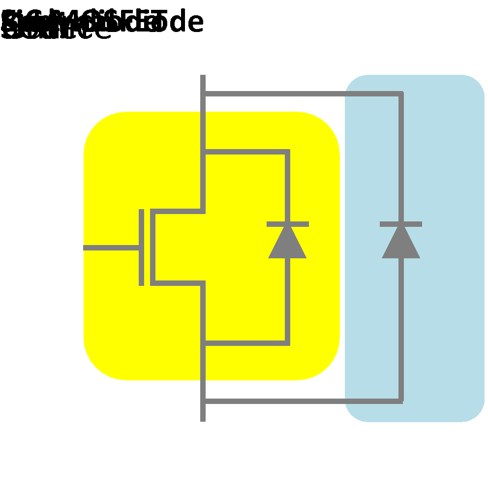
Fig. 12. Various approaches to accomplish SiC MOSFET and diode pair in a power converter application. |
||
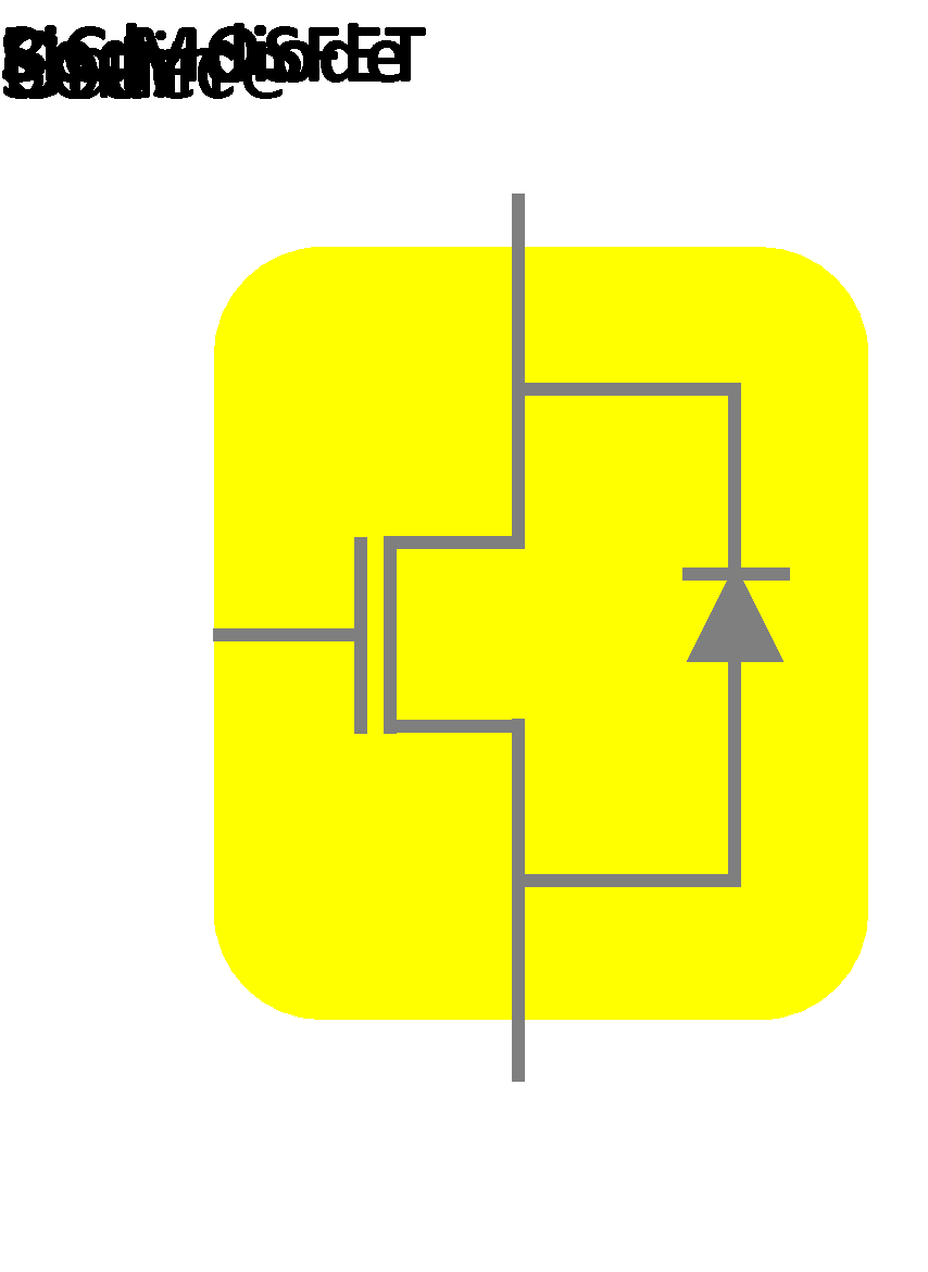
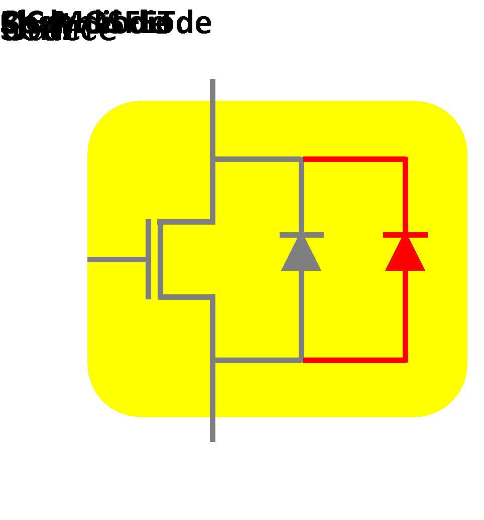
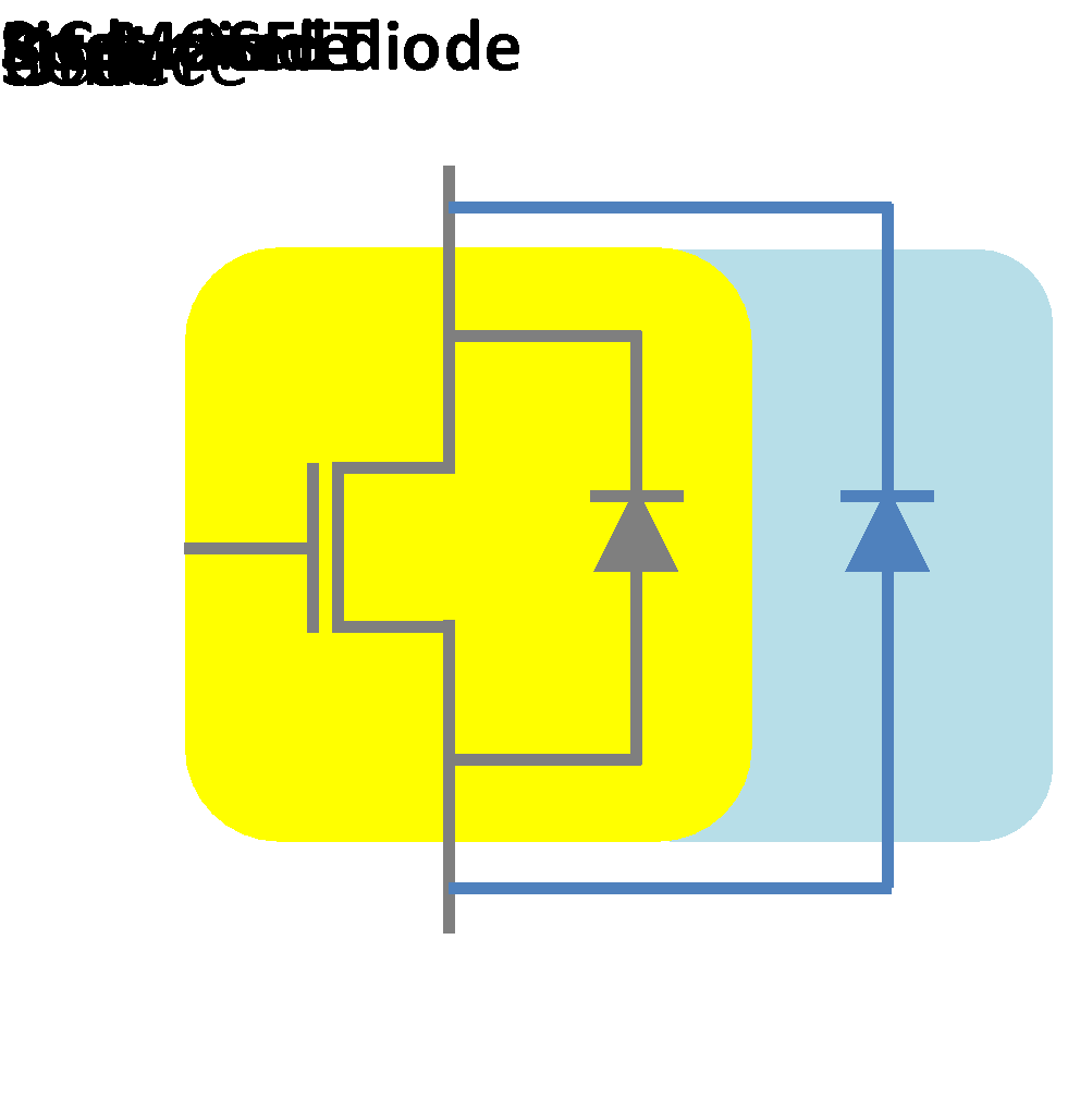
Bipolar operation of the inherent body-diode in a Silicon Carbide (SiC) MOSFET structure is undesirable for reliable device operations and reduced conduction loss. A Schottky contact based unipolar-type diode can be externally connected in parallel to a MOSFET as a separate chip in order to accommodate current in the opposite direction. In this case, the body-diode formed by the p-well and n-drift junction in the MOSFET structure will not turn-on. When a unipolar mode diode is integrated in a MOSFET structure on a single chip, it is beneficial because both MOSFET and diode not only share the forward conducting layer but they also share the edge termination region such that a significant reduction in SiC wafer area can be expected. In addition, this approach will reduce the number of packages in half bringing down the cost of implementing this technology in power converters. It will also improve efficiency and increase switching frequency by eliminating the parasitic inductance between separately packaged devices. Various approaches for a MOSFET and diode pair are summarized in Fig. 12. Panasonic proposed a MOSFET structure integrated with unipolar internal MOS-channel diode. However, since its diode structure is utilizing the MOSFET channel, and a diode requires a certain knee voltage, it is difficult to attain balanced current handling capabilities from both MOSFET and diode at the same forward voltage drops. In addition, n-epitaxial channel needs to be engineered to ensure diode current at reasonable voltage drop, which may bring issues in process latitude, and other reliability concerns in the MOSFET operation. Hestia Power Incorporation and Mitsubishi also demonstrated a MOSFET with embedded diode. In their approaches, Schottky region was formed by a separate metal process.
In this research, a simple method to accomplish a unipolar antiparallel Junction Barrier Schottky (JBS) diode functionality within the SiC MOSFET structure was proposed and experimentally verified for the first time. A simple fabrication scheme has been developed for the proposed JBSFET in order to avoid adding any processing steps to the conventional MOSFET fabrication flow.
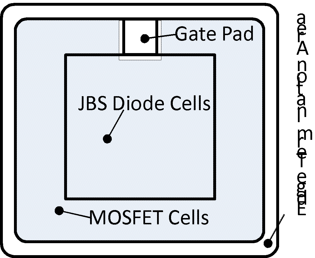
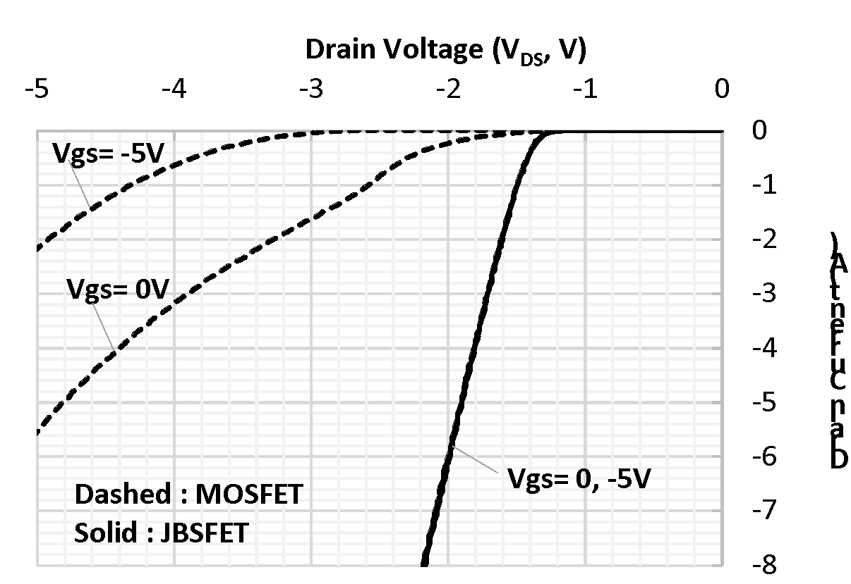
Fig. 13(a) shows the layout of the proposed SiC JBSFET. The pure JBS diode area is surrounded by MOSFET cells. It is convenient to place the MOSFET outside because the gate pad does not interrupt the big source pad, which makes the wire bonding easier, and the wire to the gate pad shorter. Area for each MOSFET and JBS diode can be determined through 2-D device simulations to target a specific current. A cross-section of the proposed SiC JBSFET is shown in Fig. 13(b). It is important to note that a single metal, single thermal treatment process was used to simultaneously form ohmic contacts on n+, p+ implanted regions, and Schottky contact on n- 4H-SiC epi-layer. Nickel (Ni) is the most commonly used metal for the ohmic contact formation on n+ region on SiC with a RTA process at higher than 950°C. Ni is also able to form an ohmic contact on p+ implanted region at the same time. However, there are no detailed reports on the formation of n- Schottky contacts simultaneously with n+ and p+ ohmic contacts. For the purpose of this work, Ni is required to remain a Schottky contact on n- epi-layer after the RTA process. Therefore, careful investigation to optimize the RTA condition was required. It was found that Ni can simultaneously form ohmic contacts on n+ and p+ implanted regions while it remains a Schottky contact on the n-epitaxial drift layer when it is annealed at moderate temperature (900°C for 2 min). Fig. 14(a) shows typical output characteristics of the fabricated JBSFET and MOSFET. As expected, the MOSFET has a lower on-resistance than the JBSFET in the forward conduction mode (first quadrant) due to the area consumed by the JBS diode. At the same active area (4.5 mm2), specific on-resistances at drain current of 1A are 7.25 mohm∙cm2 and 12.5 mohm∙cm2 for the MOSFET and the JBSFET, respectively. However, in the third quadrant, the JBSFET provides a very low forward drop due to the conduction of the JBS diode as shown in Fig. 14(b). In contrast to the MOSFET, the JBSFET shows exactly same current-voltage characteristics regardless of the gate biases. It should be noted that it is flexible to achieve a desired current in each first and third quadrant from the JBSFET by allocating appropriate area in its layout design.
 |
 |
|
(a) |
(b) |
|
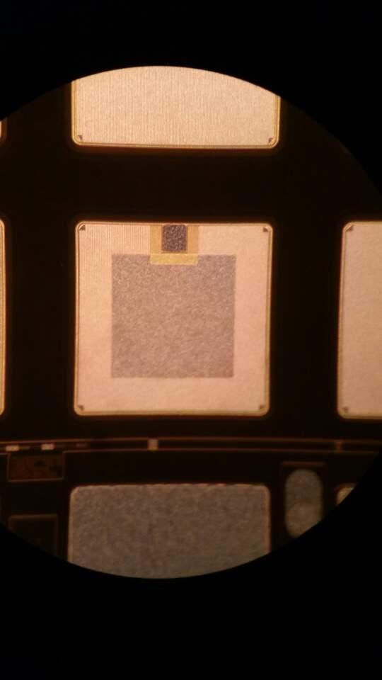
Fig. 13 (a) Schematic diagram of JBSFET layout and the chip image and (b) Cross-sectional view of JBS diode cell structure (left) and MOSFET cell structure (right). It is important to note that a single process, multi-purpose Ni contacts on 4H-SiC was used. The Schottky width is 4 µm and the cell pitch for the MOSFET is 11 µm with the channel length of 0.8 µm. |
|
 |
 |
|
(a) |
(b) |
|
Fig. 14. Comparison of (a) the first and (b) third quadrant behaviors of the fabricated JBSFET and MOSFET. The JBSFET was annealed at 900°C for 2 minutes while the MOSFET was annealed at 950°C for 2 minutes. Both JBSFET and MOSFET have the same active area: 4.5 mm2. But, in the JBSFET layout, only 45 % of the active area was allocated for the MOSFET cells. Threshold voltages for both devices are the same: 2.7V at Id=1 mA. All data were measured on wafer at room temperature. |
|
TOPIC 5: Edge termination techniques for high voltage devices on SiC [8, 9]
Conventional edge termination techniques for SiC devices include floating field rings (FFRs), junction termination extension (JTE), and modified JTE structures. Among these edge termination structures, FFRs usually require a narrow definition of the space between rings near the main p+/n junction, and tight control of defects in order to achieve the designed breakdown voltage. It is widely known that a conventional single zone JTE (SZ-JTE) is sensitive to the impurity dose resulting in a sharp peak in breakdown voltage over the JTE implant dose. The optimum JTE dose for the SZ-JTE is about 1×1013 cm-2 based on the Gauss law. To overcome this shortcoming, multiple floating zone JTE (MFZ-JTE) and space modulated JTE (SM-JTE) were proposed, which experimentally verified that high breakdown voltage can be achieved at higher dose in JTE region. Ring assisted JTE (RA-JTE) was proposed to provide high breakdown voltage with a lower JTE dose than the one optimized for the SZ-JTE.
In this research, a Hybrid-JTE that combines MFZ-JTE and RA-JTE is proposed to achieve a near ideal breakdown voltage over a wide range of JTE dose for the first time. A conventional FFR structure that consumes the same area was designed and fabricated at the same time for a comparison purpose.
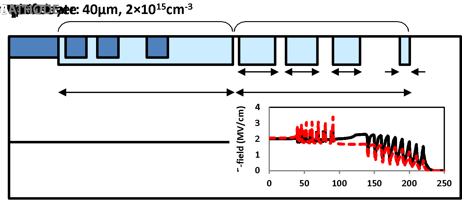
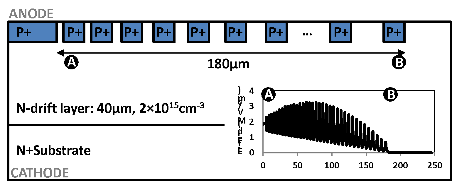
Fig. 15(a) shows the proposed Hybrid-JTE structure that simply combines a RA-JTE and a MFZ-JTE structure. 40µm thick-, 2×1015cm-3 doped drift layer was chosen to attain 5500V from a parallel plane p+n diode. 35-FFRs was also designed and optimized based on extensive 2-D simulations (Fig. 15(b)). Total width for both Hybrid-JTE and FFRs is 180 µm. Each RA- and MFZ-JTE is designed exclusively and then combined to create the proposed Hybrid-JTE structure.
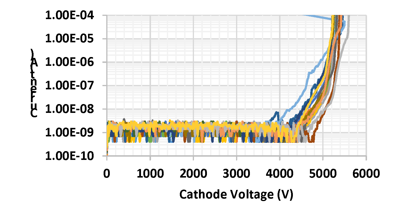
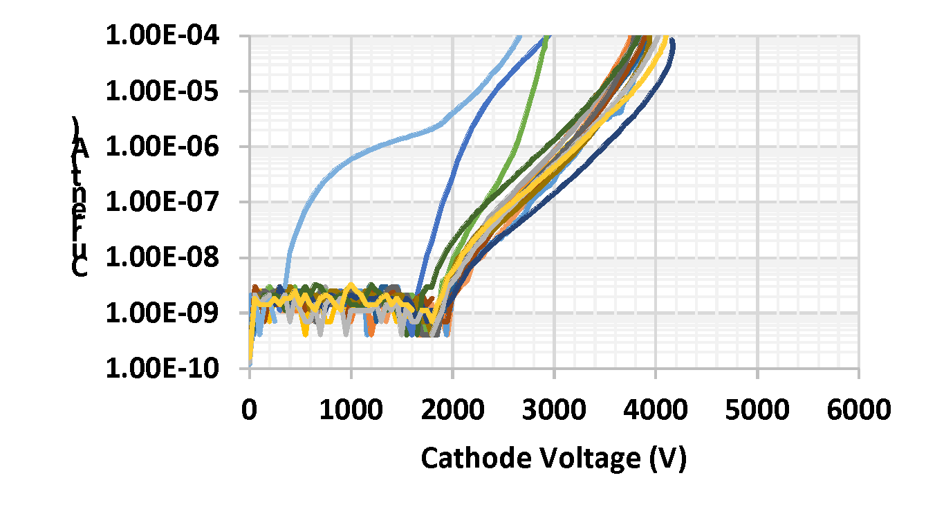
Fig. 16 shows measured reverse blocking characteristics of the fabricated PiN diodes with the proposed Hybrid-JTE structures and FFRs. The maximum breakdown voltage achieved by using the Hybrid-JTE was 5450V at anode current of 100 µA, which is 99% of the ideal value for a 1-D structure calculated using Konstantinov’s form for the critical electric field for our structure. From most of dies, the leakage current is maintained very low up to 4000V. In contrast, the maximum breakdown voltage from the PiN diode with FFRs was 4160V. Furthermore, a significant increase in leakage current is observed at relatively low voltage at ~2000V. Overall, it was experimentally demonstrated that the Hybrid-JTE provides a nearly ideal breakdown voltage with tight distribution across the wafer. In addition, wider range of JTE implant doses were allowed for achieving high breakdown voltages using the Hybrid-JTE.
 |
 |
|
(a) |
(b) |
|
Fig. 15 (a) Cross-sectional view of the proposed Hybrid-JTE structure. 6-rings are placed in the consecutive SZ-JTE to relieve electric field at location ‘A’. Exclusively optimized MFZ-JTE structure is placed next to the RA-JTE relieving electric field at location ‘B’. Rings for RA-JTE are formed by the P+ main junction implant. Discrete charge zones for MFZ-JTE and SZ-JTE region are formed by single implant process, (b) Cross-sectional view of floating field rings (FFRs) termination structure. 3µm wide 35-ring consumes 180µm in width. Simulated electric fields at the breakdown condition are shown in the insets; for the Hybrid-JTE, the dashed line indicates a low dose (9×1012 cm-2) and the solid line shows a high dose case (1.25×1013 cm-2). |
|
 |
 |
|
(a) |
(b) |
|
Fig. 16. Blocking behaviors of randomly selected 16-PiN diodes with (a) Hybrid-JTE, dose=1.8×1013 cm-2, (b) 35-FFR. |
|
Publications
- Woongje Sung, and B. J. Baliga, “Design and Economic Considerations to Achieve the Price Parity of SiC MOSFETs with Silicon IGBTs,” Materials Science Forum, Vols. 858, pp. 889-893,2016;
- Anant Agarwal, Woongje Sung, Laura Marlino, Pawel Gradzki, John Muth, Robert Ivester, and Nick Justice, “Wide Band Gap Semiconductor Technology for Energy Efficiency,” Materials Science Forum, Vols. 858, pp. 797-802,2016;
- Woongje Sung, B. J. Baliga, and Alex Q. Huang, "Area-Efficient Bevel-Edge Termination Techniques for SiC High-Voltage Devices," IEEE Transaction on Electron Devices, vol.63, no.4, pp.1630-1636, Apr. 2016;
- Woongje Sung and B. J. Baliga, “Design and Fabrication of 1400V 4H-SiC Accumulation Mode MOSFETs (ACCUFETs),” proceeding of 11th European Conference on Silicon Carbide and Related Materials, Sep. 25-29, Halkidiki, Greece, 2016
- Woongje Sung, Kijeong Han, and B. J. Baliga, “A comparative study of channel designs for SiC MOSFETs: accumulation mode channel vs. inversion mode channel,” Proceedings of International Symposium on Power Semiconductor Devices and ICs (ISPSD), 2017
- Woongje Sung and B. J. Baliga, “Monolithically Integrated 4H-SiC MOSFET and JBS Diode (JBSFET) using a Single Ohmic/Schottky Process Scheme,’’ IEEE Electron Device Lett., vol. 99, Dec. 2016. DOI: 10.1109/LED.2016.2618720
- Woongje Sung and B. J. Baliga, “On Developing One-Chip Integration of 1.2kV SiC MOSFET and JBS Diode (JBSFET),” IEEE Transactions on Industrial Electronics, Approved for publication, DOI: 10.1109/TIE.2017.2696515
- Woongje Sung and B. J. Baliga, “A Near Ideal Edge Termination Technique for 4500V 4H-SiC Devices: the Hybrid Junction Termination Extension (Hybrid-JTE),’’ IEEE Electron Device Lett., vol. 37, no.12, Dec. 2016. DOI: 10.1109/LED.2016.2623423
- Woongje Sung and B. J. Baliga, “A Comparative Study of 4500-V Edge Termination Techniques for SiC Devices,” IEEE Transactions on Electron Devices, vol. 64, Issue 4, Apr. 2017, pp. 1647-1652. DOI: 10.1109/TED.2017.2664051
