News Release: Governor Cuomo Launches Next Phase of Nano Utica
Initiative with Nearly 2,000 New Jobs Expected and Over $2 Billion
in Private Investment

For Immediate Release: 8/20/2015 Governor Andrew M. Cuomo
GOVERNOR CUOMO LAUNCHES NEXT PHASE OF NANO UTICA INITIATIVE WITH NEARLY 2,000 NEW JOBS EXPECTED AND OVER $2 BILLION IN PRIVATE INVESTMENT
ams – a Global Leader in Advanced Sensor Technologies – to generate more than 1,000 new jobs and initially invest $2 billion to support new state-of-the-art manufacturing facility
GE Global Research and SUNY Poly developing Power Electronics packaging facility, expected to create nearly 500 jobs in initial phase, ultimately growing to nearly 920 over ten years
Nano Utica initiative now projected to create more than 4,000 jobs in total over next ten years
Governor Andrew M. Cuomo today announced that global technology leader ams AG, a multinational company that creates high performance sensor solutions and analog ICs, plans to generate more than 1,000 new jobs and initially invest over $2 billion to support a cutting edge, 360,000 square foot wafer fabrication facility to be constructed at the Nano Utica site in Marcy.
Governor Cuomo also announced that GE Global Research will expand its New York global operations to the Mohawk Valley, serving as the anchor tenant of the Computer Chip Commercialization Center (QUAD C) on the campus of SUNY Polytechnic Institute’s Colleges of Nanoscale Science and Engineering in Utica. Nearly 500 jobs are expected to be created in the Mohawk Valley in the next five years from SUNY Poly, GE and affiliated corporations and another 350 in the subsequent five years.
These public-private partnerships represent the launch of the next phase of the Governor’s Nano Utica initiative, which now exceeds more than 4,000 projected jobs over the next ten years. Designed to replicate the dramatic success of SUNY Poly’s Nanotech Megaplex in Albany, NANO Utica further cements New York’s international recognition as the preeminent hub for 21st century nanotechnology innovation, education, and economic development.
“This is a transformative moment that will make a difference in peoples’ lives in the Mohawk Valley for generations to come,” said Governor Cuomo. “Over the past few years, we have worked to reverse the negative and invest in Upstate NY – and today we’re taking another huge step forward. With GE and ams joining the Nano Utica initiative, we’re seeing the region’s economy gathering momentum unlike ever before. The Mohawk Valley is beginning an economic revolution around nanotechnology, and I am excited to see the region take off and thrive, both today and in the years ahead.”
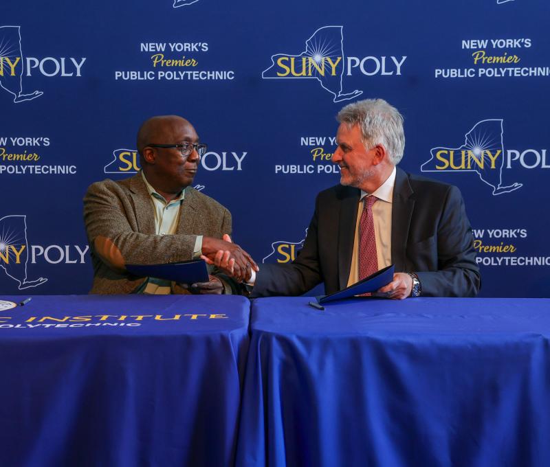
Dr. Alain Kaloyeros, President and Chief Executive Officer of SUNY Polytechnic Institute, said, "Today’s announcement by Governor Andrew Cuomo represents a major expansion for Quad-C and the Nano Utica initiative and is a tremendous victory for the Mohawk Valley and the entire State of New York. World renowned partners such as GE Global Research and AMS raise the level of prestige for the entire region and accelerate the development of this international hub for technology and innovation. Governor Cuomo’s pioneering economic development model, coupled with SUNY Poly CNSE's world class expertise and resources, continues to generate historic investment and job creation throughout the state. We welcome GE and AMS and their leadership teams and look forward to their partnership in the continued growth of Nano Utica."
ams | State-of-the-Art Manufacturing Facility
In partnership with New York State, SUNY Poly CNSE, Fort Schuyler Management (FSMC) and Mohawk Valley Edge, ams will construct, staff and operate a state-of-the-art 200/300 mm wafer fabrication facility in support of the company’s high performance analog semiconductor operations.
Construction of the ams fab is scheduled to begin in spring 2016 at the 450-acre Marcy Nanocenter site. Capital purchases, operating expenses and other investments in the facility over the first 20 years are estimated at more than $2 billion. ams will create and retain more than 700 full time jobs and anticipates the creation of at least 500 additional support jobs from contractors, subcontractors, suppliers, and partners necessary to establish the full ecosystem necessary to enable advanced manufacturing operations.
ams Chief Operating Officer Dr. Thomas Stockmeier said, “Building a new wafer fab will help us achieve our growth plans and meet the increasing demand for our advanced manufacturing nodes. Our decision to locate the facility in New York was motivated by the highly-skilled workforce, the proximity to esteemed education and research institutions, and the favorable business environment provided by Governor Cuomo and all the public and private partners we are working with on this important project.”
ams, which maintains locations in over 20 countries, chose to expand its manufacturing capabilities in New York State as a result of New York’s continued leadership in technology innovation and the opportunity to access SUNY Poly CNSE’s world class expertise and infrastructure, as well as Governor Cuomo's successful public-private partnership model and aggressive business development incentives.
Additionally, ams will collaborate with FSMC and SUNY Poly on a joint development program to support complimentary research, commercialization and workforce training opportunities at SUNY Poly facilities throughout New York State, expanding and enhancing the ever-growing high tech cluster that is centered in Albany at SUNY Poly CNSE.
GE Global Research | Power Electronics Packaging Facility
GE Global Research and SUNY Poly will develop a Power Electronics packaging facility at QUAD C that will advance New York’s leadership in next-generation semiconductor research, development, and commercial fabrication to meet the global demand for smaller, faster, and more efficient devices. This will expand the scope of the Nano Utica initiative from computer chip commercialization into power electronics applications for industrial products such as wind turbines, utility-scale solar inverters, data centers and hybrid cars. GE’s silicon carbide technology is a new material platform upon which the next generation of power devices will be built, enabling higher power in smaller, more efficient packages.
Mark Little, Senior Vice President and Chief Technology Officer of GE, said,"Together with New York State and SUNY Polytechnic Institute in Albany, and now Utica, we are creating a Silicon Carbide Corridor that will be the epicenter of the next revolution in power. In Utica, it will expand the focus from computer chip commercialization to creating the first U.S. based Power Electronics Manufacturing Center with GE's silicon carbide technology. We want to commend Governor Cuomo and Dr. Kaloyeros for providing the spark that will attract many other great companies and jobs for the Mohawk Valley."
Advanced packaging technologies are vital in the development of faster and more powerful computer chips, as well as silicon carbide chips for power electronics applications. They refer to the conductors that connect the circuits, provide power, and discharge heat to keep the chips functioning properly. The packaging facility at QUAD C will lead to commercial breakthroughs in an array of applications ranging from defense, super-computing, tablets, cell phones, and a myriad of power electronics applications.
The packaging facility is a critical component of the New York Power Electronics Manufacturing Consortium, the governor’s $500 million public-private semiconductor research partnership that includes over 100 companies. Based at the SUNY Poly Megaplex in Albany with lead partners including GE and IBM, the Consortium is driving coordinated materials research and job creation across the Upstate corridor.
Oneida County Executive Anthony J. Picente, Jr. said,“Thanks to the Governor’s support and the Nano Utica project, Oneida County is well on its way to a healthier and more vibrant economy. This particular project exemplifies what we can do when the private sector takes notice of everything the Mohawk Valley has to offer. I am proud to develop the partnership we have made with the state and together, we will continue to focus on the issues that matter most for Oneida County and the Mohawk Valley region.”
Utica Mayor Robert Palmieri said, “The Nano Utica initiative is revolutionizing the local economy, bringing global companies, billions of dollars in private investment, and thousands of jobs to our region. That’s something I couldn’t have even imagined a decade ago, and it’s thanks to Governor Cuomo that we have this tremendous project taking shape in our own backyard. I’m thrilled to see Nano Utica moving forward, and am excited to continue partnering with the Governor and our state partners to keep Utica’s economy growing.”
Senator Joseph A. Griffo said,“Today, the Mohawk Valley takes its next big step into the future of the 21st century. As we welcome the new partnership of G.E. and ams Technologies with SUNY Polytechnic Institute in Marcy, we look forward to the potentially historic economic transformation that such an opportunity could bring to our region as a leader in nanotechnology. The quality jobs, further investment and growth that this announcement promises can only help make our region bigger and better, and we commend the Governor for his strategic vision in recognizing all we had to offer in this endeavor. And to all the local, county and state leaders who never lost faith as a collective team that this day would come, we thank you for your perseverance.”
Assemblyman Anthony J. Brindisi, said,“I am thrilled to welcome the next phase of the Nano Utica initiative. This is another massive step forward for our community – one that builds on the progress that we have already seen and brings more than a thousand additional jobs to the region. Governor Cuomo has zeroed in on the needs of communities like Utica for going on five years now – and this is another tremendous example of what we can accomplish with his support and our collective potential.”
Mohawk Valley EDGE President Steve DiMeo said,“The Nano Utica project has brought together the best and brightest minds with some of the world’s most cutting-edge and competitive companies. Today was about prioritizing the needs of this region and that is exactly what the Governor and his staff did. We have seen a transformation in the Mohawk Valley and after participating in today’s discussions, I am confident the progress will not stop there.”
Nano Utica
Nano Utica is Governor Cuomo’s $1.5 billion economic development blueprint to revitalize the Mohawk Valley by establishing a dynamic nanotechnology-driven ecosystem by replicating the tremendous success of SUNY Poly’s College of Nanoscale Science and Engineering in Albany and includes QUAD C and the Marcy Nanocenter. The expansion of QUAD C includes state-of-the-art cleanrooms, laboratories, hands-on education and workforce training facilities, and integrated offices encompassing 253,000 square feet. The cleanroom will be the first-of-its-kind in the nation: a 56,000 square-foot cleanroom stacked on two levels that is now five times larger than initial plans.
In accordance with the governor’s innovation-driven economic development model, no public funds will be given to private companies. New York will invest $250 million at QUAD C and the Marcy Nanocenter to support critical equipment and infrastructure improvements at both locations. The state will own and manage these facilities through SUNY Poly and such state investment will catalyze the Mohawk Valley’s high-tech economic ecosystem, attracting additional nanotechnology jobs and supply chain companies to support and contribute to Nano Utica initiative.
###
Additional news available at www.governor.ny.gov New York State | Executive Chamber | press.office@exec.ny.gov | 518.474.8418

