Nikon News Release: Nikon Announces 450 mm ArF Immersion Scanner at SUNY Polytechnic Institute is Transitioning to Wafer Patterning
Published:
Thursday, July 9, 2015 - 13:28

[caption id="" align="alignright" width="352"] 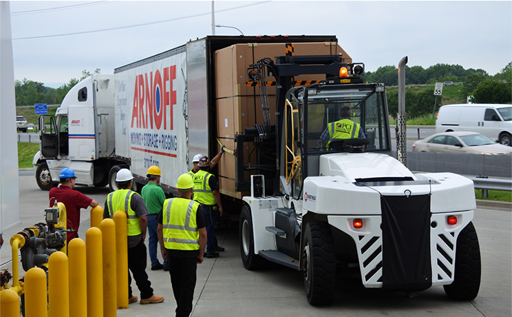 Delivery of ArF Immersion Scanner NSR-S650D[/caption]
Nikon Corporation (Kazuo Ushida, President) announced the world's first ever 450 mm immersion scanner, the Nikon NSR-S650D, has been installed at SUNY Polytechnic Institute's Colleges of Nanoscale Science and Engineering (SUNY Poly CNSE) and is transitioning to wafer patterning. This milestone is a significant achievement in accelerating development of the next generation of computer chips.
In July of 2013, Nikon announced it had entered into a partnership with SUNY Polytechnic's College of Nanoscale Science and Engineering to develop next generation 450 mm photolithography technology. In April of this year, Governor Andrew M. Cuomo announced installation of the world’s first ever 450 mm immersion scanner had begun at the SUNY Polytechnic Institute's Albany NanoTech Complex.
Toshikazu Umatate, General Manager of the Nikon Corporation Semiconductor Lithography Business Unit said, "Our 450 mm program is advancing well. The NSR-S650D shipped earlier this year as planned, and we will transition to wafer patterning soon. The program's steady progress is a direct result of tireless collaborative efforts across the 450 mm consortium." Umatate added, "Nikon is dedicated to supporting the industry's drive to next generation semiconductor manufacturing through continuous innovations in lithography system performance and productivity."
“As a testament to Governor Andrew M. Cuomo’s leadership making New York State the epicenter for globally recognized high-tech research, development, and commercialization, the installation of the world’s first Nikon 450 mm immersion scanner and its deployment for wafer patterning inside SUNY Poly CNSE’s state-of-the-art cleanroom facilities is a milestone for the Global 450mm Consortium, and it proves that the industry’s transition to the 450 mm platform technology is gaining further momentum,” said Paul Farrar, Jr., General Manager of the Global 450 mm Consortium (G450C) and CNSE Vice President for Manufacturing Innovation. “Governor Cuomo’s strategic, high-tech investments are enabling the industry’s transition to 450mm wafer technology, and we are proud that, as a result, this latest development is yet another that is taking place in New York State. Through the Governor’s leadership and foresight, this game-changing initiative continues to drive progress, as well as career and business opportunities, laying the foundation for advanced technologies that will power innovation far into the future.”