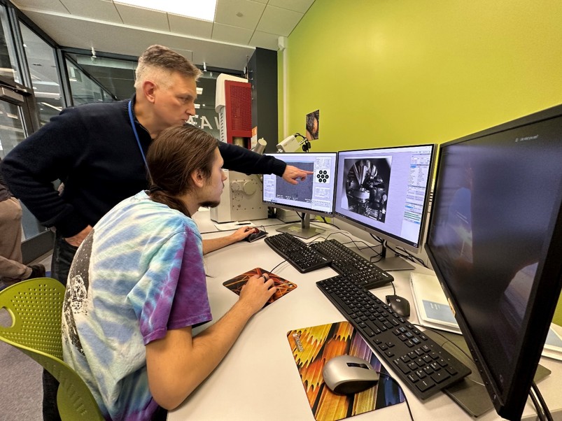
SUNY Polytechnic Institute is taking a major step forward in advancing semiconductor innovation with the upcoming Semiconductor Processing to Packaging Center. This state-of-the-art facility will serve as a hub for research, education, and collaboration, supporting next-generation technologies in power electronics, optoelectronics, and clean energy applications.
Key Highlights
- $16 Million Investment from New York State to establish the Processing-to-Packaging Center.
- $4 Million ESD Grant dedicated to a full suite of advanced metrology equipment.
- $6.5 Million Pending for outfitting the facility and providing scholarships and student support.
Facility Features
- Approximately 5,000 ft² of cleanroom space for advanced device processing.
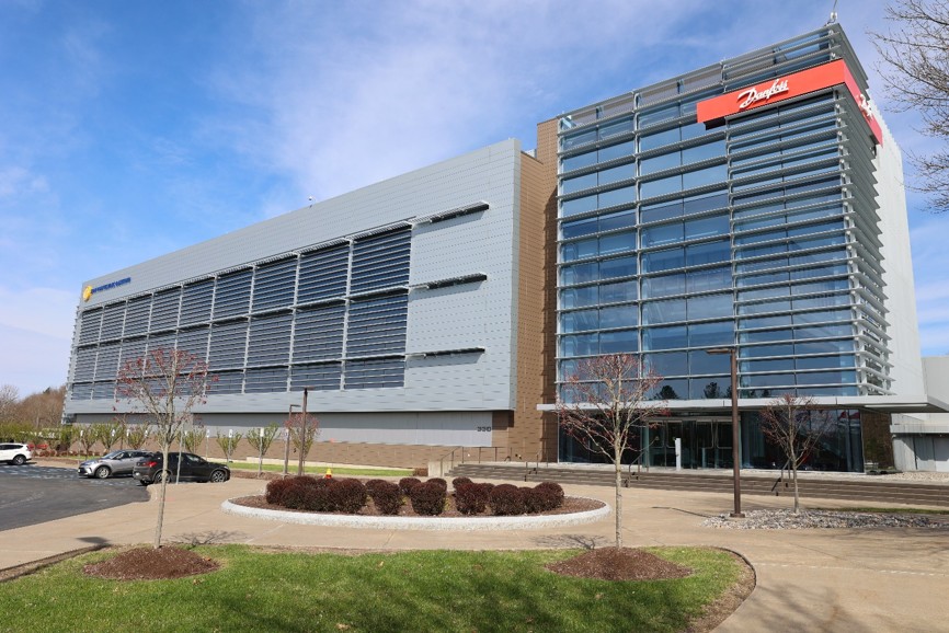
- Two 30-seat lecture classrooms located in the Quad C / Semikron-Danfoss building.
- Capability to process silicon devices as well as SiC, GaN, AlN and their alloys, and Ga₂O₃ devices, addressing unique packaging needs for each.
Impact and Vision
The Center will enable cutting-edge research and development for:
- Power electronics
- Optoelectronics
- Clean energy applications
SUNY Poly is also committed to developing a robust research ecosystem through partnerships with regional, state, and national collaborators, fostering innovation and workforce development in the semiconductor industry.
