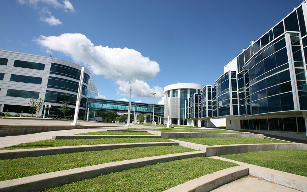
Learn more about SUNY Poly's Albany NanoTech Complex
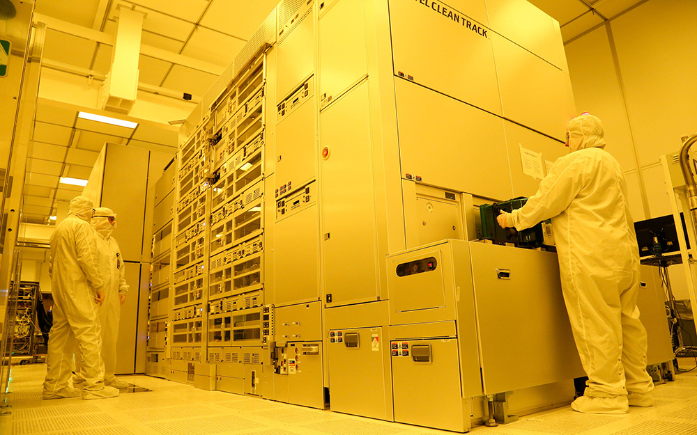
SUNY Poly's 80,000 square feet of fabrication facilities located at its Albany NanoTech Complex house more than 120 wafer processing and inline metrology tools. The tool sets installed in SUNY Poly's world-class facilities are dedicated to supporting the industry's wafer processing needs for the next several device generations ranging from 65nm to 15nm, and allowing exploratory work in support of full scaled nanotechnology.
SUNY Poly's next-generation facilities are currently operational with a fully enabled 65nm low power CMOS and RF CMOS offering. Early user hardware, custom R&D and on-demand derivative development support is provided at SUNY Poly with access to unique state-of-the-art industry standard semiconductor fabrication facilities, which serves as a technology test-bed leading to the development, demonstration, integration and qualification of advanced fabrication technologies for the semiconductor industry.
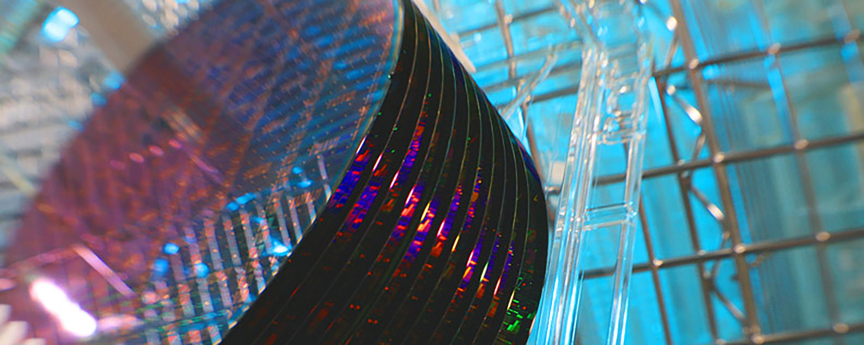
The SUNY Poly facilities house 300mm advanced lithography platforms to support 193nm immersion lithography development and EUV lithography development. Also installed are advanced wafer platforms for planarization, copper plating, etch development, ion implantation, thin film development and wet cleaning technology. Our service offerings include but are not limited to, Lithography Services, Film Deposition, CMP, Etch Services, Mask Sets, Derivatives, Hot Processes, Metals, Wets, Implants and Material Analytical Services.
Learn about 300mm wafer fabrication