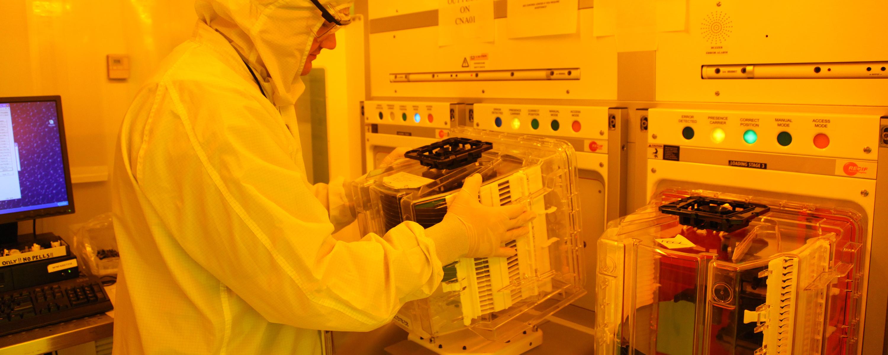
Product qualification support is provided at SUNY Poly with access to a unique state-of-the-art industry standard semiconductor fabrication facility, which serves as a technology test-bed leading to the development, demonstration, integration and qualification of advanced fabrication technologies for the semiconductor industry.
SUNY Poly's Albany NanoTech Complex includes NanoFab Central, a 100,000-square-foot building that houses 15,000 square feet of 300mm wafer, class 1 capable cleanroom space, and NanoFab East, a separate 250,000-square-foot office, laboratory and classroom building.
The 35,000 square feet of cleanroom space in NanoFab North is dedicated to supporting the nanoelectronic industry's advanced R&D needs. The tool sets installed in these new facilities are dedicated to supporting the industry's 300mm wafer processing needs for the next several device generations including 65nm, 45nm, 32nm and 22nm through the full transition to nanotechnology.
NanoFab North houses several 300mm wafer process tools including advanced lithography platforms to support 193nm immersion lithography development and EUV lithography development. Also installed are advanced 300mm wafer platforms for planarization, copper plating, etch development, ion implantation, thin film development and wet cleaning technology.
The NanoFab South technology acceleration facility provides space for business incubation, SUNY Poly classrooms, workforce training, offices, and large and small industrial sponsors and partners including IBM, TEL, Applied Materials and ASML. The facility includes 32,000 square feet of cleanroom to support these partners and other next generation nanotechnology research activities.


