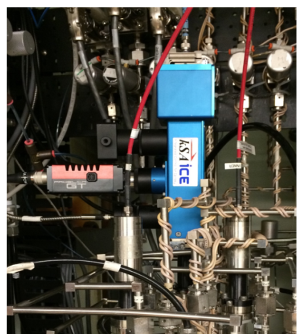
MOCVD equipped with k-space in situ stress evolution/growth monitoring system
Thickness Monitoring
- Reflectance measured during growth
- Changes in reflectance used to determine material thickness and growth rate
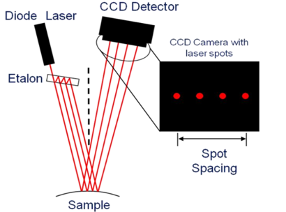
Stress Monitoring
- Curvature of wafer measured using laser array
- Stress calculated using Stoney Equation to monitor real-time stress evolution during growth
 |
 |
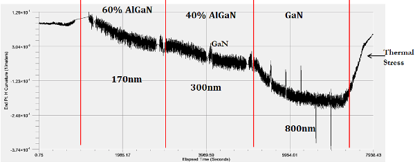 |
| Schematic of laser array used to measure wafer bowing | k-space ICE tool mounted on D180 | Wafer curvature/stress evolution during the growth of GaN on Si(111) |